RCV
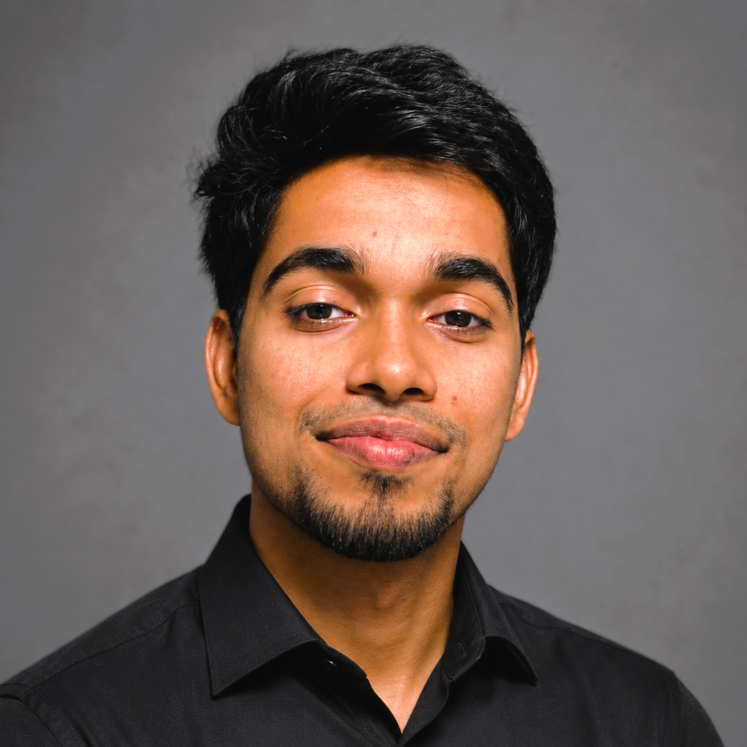
Rahul Chembra Vasudevan

Rahul Chembra
Vasudevan

Researcher in diamond integrated photonic platforms, building scalable nanofabrication and packaging workflows for industrial quantum sensors.

cvrahul40@gmail.com LinkedIn Rennes, France
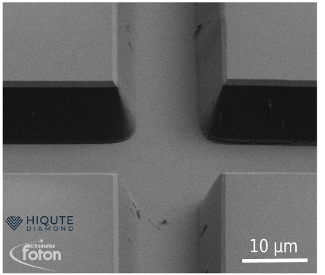
Deep etching of Single crystal diamond beyond 15 um
Diamond pillars
Deep ICP-RIE etch of Single Crystal Diamonds· upto 30 µm · 4 nm sidewall roughness (AFM)
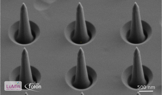
Diamond nanopillars for Neuronal imaging
SEM etching
Diamond pillars · 200 nm · NV membrane . Neuronal imaging
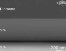
Room-temperature bonded diamond-on-silica heterostructure
Bonded membrane
Room-temp bonding · diamond on silica
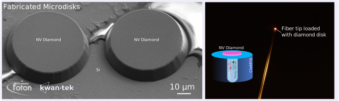
Fiber endoscope for NDT using um scale NV diamonds/
Optical setup
Industrial Fiber endscope· Micromanaipulation and pacakaging · For NDT solutions
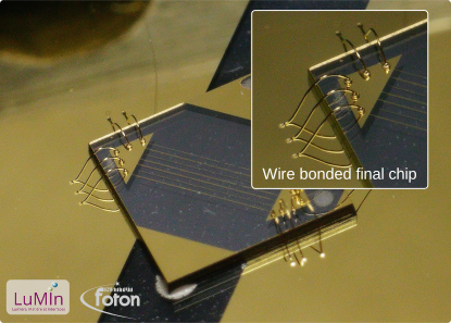
Diamond chip for electrometry
Packaged device
Diamond chip for electrometry

I work on scalable fabrication of diamond integrated photonic platforms for industrial quantum sensing.

With major expertise in designing cleanroom fabrication workflows (lithography, thin film depositions, plasma etching), membrane bonding and packaging, and building custom optical characterization setups for integrated photonic devices for quantum sensing.

Apart from research, I enjoy creating and showcasing various artworks, ranging from digital illustration (Blender, Inkscape) to acrylic paintings and pencil drawings, with several exhibitions conducted. I love to transfer my creative side into my scientific communications as well.

Currently open to photonics R&D and process engineering roles where cleanroom skills and optical characterization are valued for industrial research and manufacturing.

PhD, Photonics
Institut Foton · INSA Rennes · University of Rennes, France
Photonic integration of diamond materials for NV ensemble based quantum sensing
2024 – Present
M2 Photonics, Optical Communication — Exchange Student
ENSSAT, University of Rennes, France
2022 – 2023
Integrated M.Sc., Photonics
Cochin University of Science and Technology, India
2018 – 2023

PhD — Diamond Integrated Photonics

2024 – Present
Institut Foton, INSA Rennes, France
Established the lab's first diamond nanoprocessing and packaging workflows, together with device characterisation setups. Key results: fabricated high-aspect-ratio pillars down to 200 nm diameter for neuronal electrometry; achieved deep etching of single-crystal diamond up to 30 µm with 3 nm sidewall roughness; developed a room-temperature bonding process for diamond membranes for integrated photonics; and integrated micrometre-scale diamond membranes with optical fibers for an industrial prototype of non-destructive-testing endoscope.

Master Thesis — Quantum Optics

2022 – 2023
Institut Foton, University of Rennes, France
Built NV magnetometry setups and developed a quantum optics practical course based on entangled photon pair generation via SPDC in BBO crystals. The course included demonstrations of Bell's inequality violation, Hong–Ou–Mandel interferometry, and second-order correlation measurements.

Mitacs Globalink Fellow

May – Jul 2022
TRIUMF Particle accelerator center, Vancouver, Canada
Simulated multi-step laser ionization of Rb and Na using density-matrix simulations, validated against photoionization data from the ISAC (Isotope Separator and Accelerator) beamline.

Industrial Project Student

Jun – Aug 2021
IIT Kanpur, India
Trained ML models for diabetes detection (classical pipeline) and human iris classification (CNN).
Diamond and Related Materials · Vol. 168 · 2026 · Article 113992
Scalable fabrication of diamond-on-silica heterostructures via high-selectivity deep ICP-RIE and room-temperature bonding
R. Chembra Vasudevan, A. Hammouti, J. Le Pouliquen, T. Batte, P. Pirasteh, Y. Dumeige, P. Huillery
View on ScienceDirect ↗

Cleanroom Skills

Photolithography E-beam Lithography ICP-RIE RIE PECVD Sputtering E-beam Evaporation

Fabrication & Packaging

Diamond Membrane Bonding Fiber Endoscope Packaging Wire Bonding

Characterisation

NV-Center Magnetometry Quantum-grade diamond characterization AFM SEM Ellipsometry Raman Spectroscopy Photonic Integrated Circuit Characterisation

Simulation & Design

COMSOL KLayout MATLAB Python Inkscape Blender
Art
Art
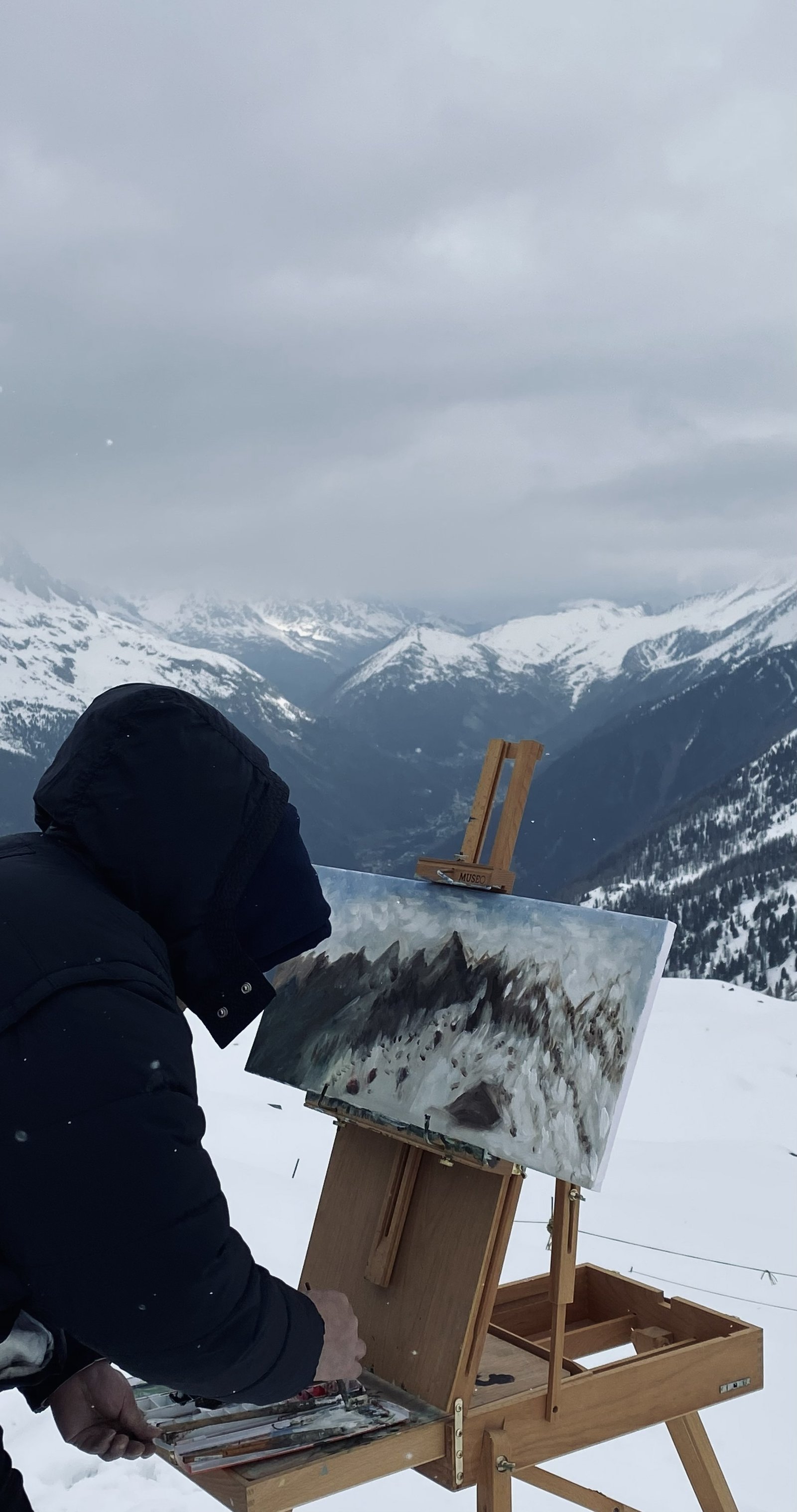
Art (Painting at Chamonix)
Cooking
Cooking
Cooking (Choclate Brownie with Blueberries)
Hiking
Hiking
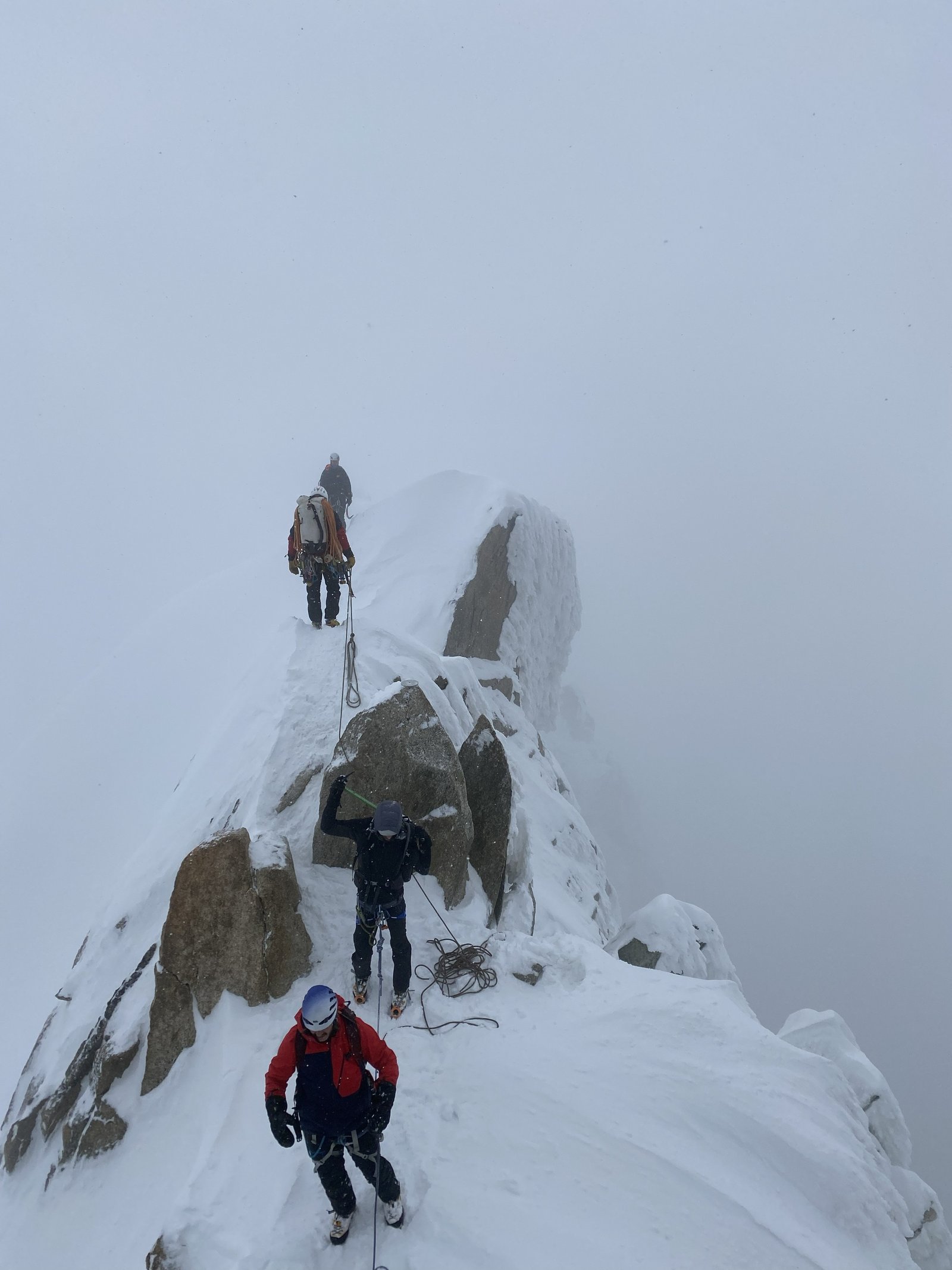
Hiking (Mont Blanc Alps)
Science communication
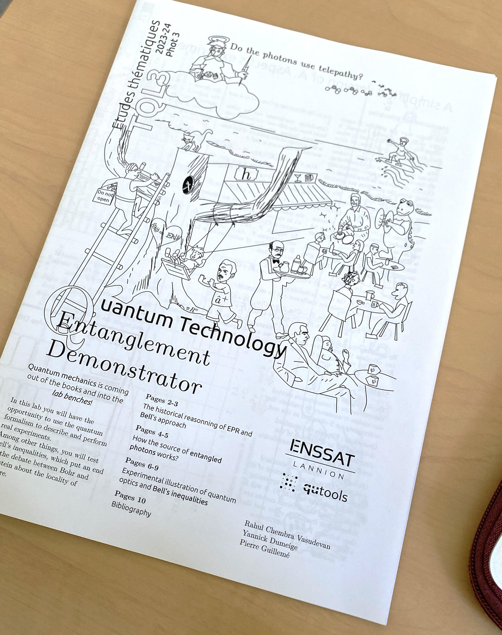
Science communication. illustartion
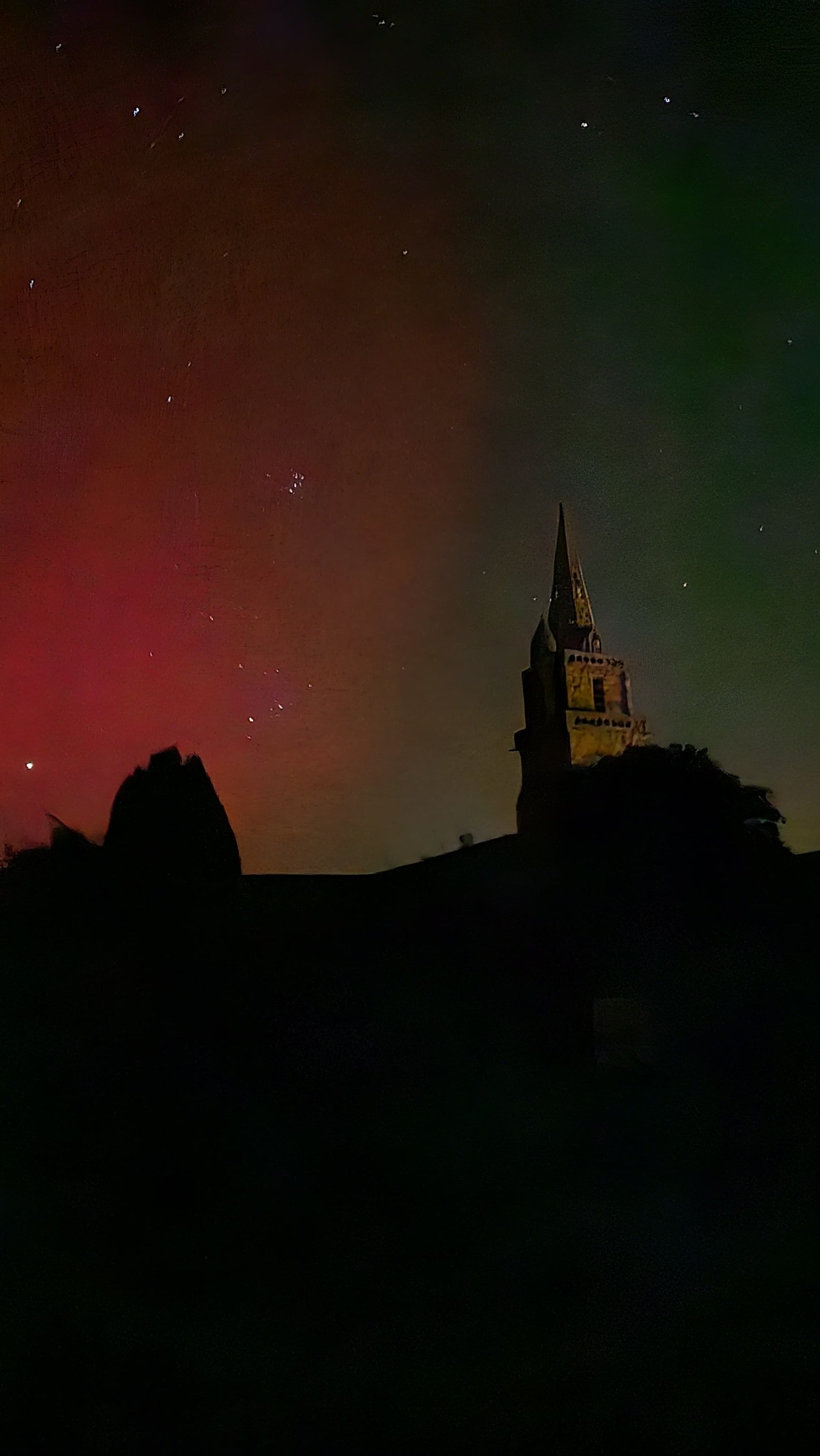
Photograph
Photography
Photography (Aurores boréales at Lannion, Bretagne)
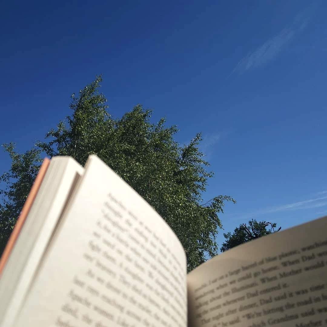
Reading
Reading
Reading

Open to photonics R&D, process engineering, and quantum application roles.

cvrahul40@gmail.com · Download CV